 杭州米乐M6纳米科技有限公司
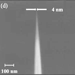
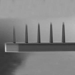
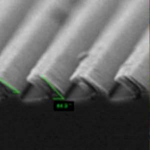
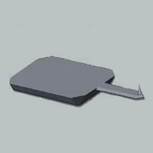
AFM探针 AFM Probe
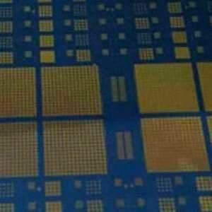
代工结构/器件 OEM Structure/Device
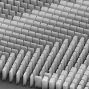
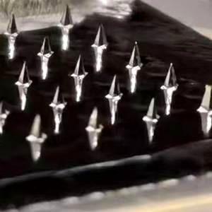
AFM探针,电子束曝光,纳米压印,激光直写(无掩膜光刻),真空镀膜,溅射镀膜,PECVD,LPCVD,ICP-RIE,深硅刻蚀,金属刻蚀,介质刻蚀,离子束刻蚀,微针,AR/VR/MR斜齿/闪耀光栅,超构透镜(单晶硅,非晶硅,氮化硅),硅光结构,深硅/体硅结构,等 AFM Probe, Electron Beam Lithography, Nanoimprinting, Laser Direct Writing(Maskless Lithography), Vacuum Deposition、Sputtering, PECVD, LPCVD, ICP-RIE, Deep Reactive Ion Etching, Metal Etching Medium Etching, Ion Beam Etching, Microneedle, AR/VR/MR Slanted/Blazed Gratings, Metalens(Monocrystalline Silicon, Amorphous Silicon, Silicon Nitride), Silicon Optical Structures, Deep Silicon/Bulk Silicon Structures, etc

杭州米乐M6纳米科技有限公司成立于2016年4月份,是国内首家从事AFM探针研发、生产、销售的公司,同时提供微纳加工工艺咨询与服务及微纳领域的新产品研发。
Hangzhou Tanzhen NanoTech Co., Ltd.,founded in April 2016, is the first company in China to engage in the research, produce and sales of AFM probe, as well as to provide micro-nanofabrication process consulting and services and new product development in the field of micro-nano.
公司的发展目标是打造成全球有竞争力的全品类AFM探针生产厂商和MEMS综合代工代研平台。
The company’s development goal is to become a globally competitive manufacturer of a full range of AFM probes and a comprehensive MEMS OEM and R&D platform.
公司的创始人崔波教授,本科毕业于北京大学物理系,博士毕业于美国普林斯顿大学电子工程系,后在加拿大国家实验室任职多年,现任加拿大滑铁卢大学电子与计算机工程系终身正教授,并担任该校微纳加工中心主任。具有27年的微纳米加工研究经验和14年的项目团队管理经验。
The founder of the company, Professor Bo Cui , graduated from the Department of Physics of Peking University as an undergraduate, and graduated from the Department of Electrical Engineering of Princeton University as a Ph.D., and then worked at the National Laboratory of Canada for many years, and is now a tenured full professor in the Department of Electrical and Computer Engineering at the University of Waterloo, Canada, and the director of the micro and nano-processing centre of the same university. He has 27 years of experience in micro- nanofabrication research and 14 years of experience in project team management.
由原中科院微电子所研究员朱效立博士领衔的,来自于加拿大滑铁卢大学的博士、硕士、中科院物理所及上海大学的硕士研发技术团队,目前共十四人,全部为硕士以上学历。米乐M6与加拿大滑铁卢大学、清华大学、上海交通大学、南京大学、中科院苏州纳米技术与纳米仿生研究所等多家微纳领域海内外学术及研发机构,均有深度合作。
Led by Dr Xiaoli,Zhu , former researcher of the Institute of Microelectronics of the Chinese Academy of Sciences, the R&D technical team from the University of Waterloo (Canada) with PhDs and Masters, and the Institute of Physics CAS and Shanghai University with Masters, is currently composed of 14 people, all of whom with Masters or above degrees. The company has deep cooperation with many academic and R&D institutions in the field of micro and nano, such as University of Waterloo, Tsinghua University, Shanghai Jiao Tong University, Nanjing University, Suzhou Institute of Nano-Tech and Nano-Bionics,CAS, and other domestic and overseas academic and R&D institutions.
公司目前已在山东淄博建立起了包括激光直写,深硅刻蚀,低温刻蚀等二十多台设备,总价值超过2000万元的百级超净间。
The company has now established a 100-class ultra-clean room in Zibo, Shandong Province, which includes more than 20 sets of equipments including laser direct writing, Deep Reactive Ion Etching, low temperature etching, etc., with a total value of more than 20 million yuan.
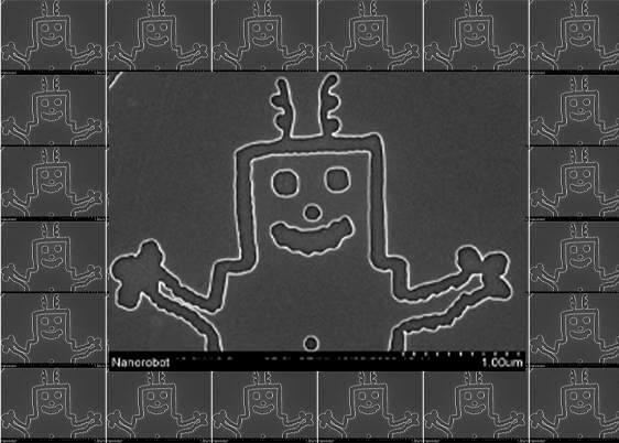
公司自主开发及代研了二十多项产品和项目,获得五项技术专利。所研发的原子力显微镜大高宽比探针等一系列原子力显微镜探针产品,填补了国内空白,可实现国产替代,解决卡脖子问题。
The company has developed and researched more than 20 products and projects on its own, and obtained five technology patents. A series of atomic force microscope probe products, such as the high aspect ratio probe of atomic force microscope developed by the company, have filled the gaps in the country, and can realise the domestic substitution and solve the stranglehold problem of nano field in china.
公司为海内外多家单位,在微针、AR/VR/MR斜齿/闪耀光栅、超构透镜(单晶硅、非晶硅、氮化硅)、硅光机构、深硅/体硅结构等等器件与机构方面,提供过代工代研服务。
The company has provided OEM and R&D services for a number of units at home and abroad in the areas of microneedles, AR/VR/MR Slanted/Blazed Gratings, Metalens (monocrystalline silicon, amorphous silicon, silicon nitride), silicon optical mechanisms, deep silicon/bulk silicon structures, and other devices and institutions.
国际领先的先进工艺和多年的丰富经验
在对传统的AFM探针加⼯⼯艺的研究基础上,团队不断进⾏加⼯⽅法与⼯艺的改良与迭代
历经15年专注的研究与实践,从⼯艺⽅案、设备适配度、⼯艺参数(⽐如刻蚀⽓体⽐例功率压强)等各个加⼯环节,都积累了成熟的经验
在AFM探针加⼯技术与⼯艺领域始终保持着技术领先性与时间层⾯上的技术护城河
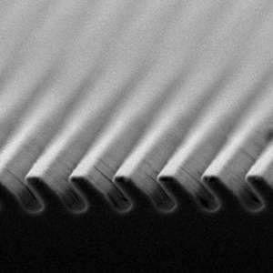
MEMS加⼯技术(尤其是硅⼲法刻蚀技术)已经取得⻓⾜进展,可控性好效率⾼,且成本在不断降低。项⽬核⼼技术就是利⽤⼤批量MEMS加⼯技术来替代传统的探针加⼯技术,直接批量制造出⾼端探针。
· news ·
米乐M6新闻与行业动态
紧跟技术发展,了解行业动向


提交咨询信息
咨询热线:0731-1234567
米乐M6收到后将会在24小时内回复您